- 您现在的位置:买卖IC网 > Sheet目录1997 > ICS81006AKLFT (IDT, Integrated Device Technology Inc)IC VCXO TO 6 LVCMOS OUT 20VFQFPN
VCXO-TO-6 LVCMOS OUTPUTS
ICS81006
IDT / ICS VCXO-TO-LVCMOS OUTPUTS
1
ICS81006AK REV. B OCTOBER 8, 2008
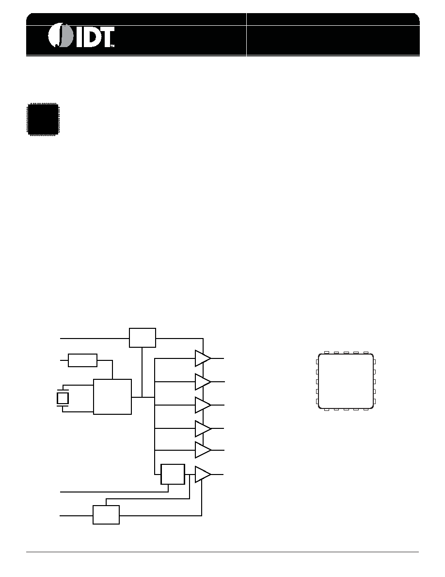
VCXO
0: ÷1
1: ÷2
SYNC
LP Filter
GENERAL DESCRIPTION
The ICS81006 is a high perfor mance, low jitter/
low phase noise VCXO and is a member of the
HiPerClockS family of high performance clock
solutions from IDT. The ICS81006 wo r ks in
conjunction with a pullable cr ystal to generate
an output clock over the range of 12MHz - 31.25MHz and
has 6 LVCMOS outputs, effectively integrating a fanout
buffer function.
The frequency of the VCXO is adjusted by the VC control
voltage input. The output range is ±100ppm around the
nominal crystal frequency. The VC control voltage range is
0 - V
DD. The
device is packaged in a small 4mm x 4mm
VFQFN package and is ideal for use on space constrained
boards typically encountered in ADSL/VDSL applications.
FEATURES
Six LVCMOS/LVTTL outputs, 20Ω nominal output impedance
Output Q5 can be selected for ÷1 or ÷2 frequency relative to
the crystal frequency
Output frequency range: 12MHz to 31.25MHz
Crystal pull range: ± 90ppm (typical)
Synchronous output enable places outputs in High-Imped-
ance state
On-chip filter on VIN to suppress noise modulation of VCXO
V
DD/VDDO combinations
3.3V/3.3V
3.3V/2.5V
3.3V/1.8V
2.5V/2.5V
2.5V/1.8V
4mm x 4mm 20 Lead VFQFN package is ideal for space
constrained designs
0°C to 70°C ambient operating temperature
Available in both standard (RoHS 5) and lead-free (RoHS 6)
packages
HiPerClockS
ICS
BLOCK DIAGRAM
PIN ASSIGNMENT
OE0
VC
XTAL_IN
XTAL_OUT
DIV_SEL_Q5
OE1
Q0
Q1
Q2
Q3
Q4
Q5
(Pullup)
(Pulldown)
XTAL_IN
XTAL_OUT
VDD
VC
DIV_SEL_Q5
GND
Q2
VDDO
Q3
GND
OE1
GND
Q5
V
DDO
Q4
OE0
GND
Q0
V
DDO
Q1
1
2
3
4
5
20 19 18 17 16
ICS81006
20-Lead VFQFN
4mm x 4mm x 0.925 package body
K Package
Top View
6
7
8
9
10
15
14
13
12
11
(Pullup)
发布紧急采购,3分钟左右您将得到回复。
相关PDF资料
ICS810525AGILF
IC VCXO-LVCMOS/LVTTL 16-TSSOP
ICS813076CYILF
IC VCXO-PLL WIRELESS 64-TQFP
ICS813078BYILF
IC VCXO PLL WIRELESS 64TQFP
ICS813323BGLF
IC ATTENUATOR/MULTIPLIER 24TSSOP
ICS840002AGLF
IC FREQ SYNTHESIZER 16-TSSOP
ICS840022AKI-02LF
IC CLOCK GENERATOR 16VFQFPN
ICS84021AYLF
IC SYNTHESIZER HIGH FREQ 32-LQFP
ICS840245AGILF
IC FREQ SYNTHESIZER 16-TSSOP
相关代理商/技术参数
ICS81006AKT
制造商:ICS 制造商全称:ICS 功能描述:VCXO-TO-6 LVCMOS OUTPUTS
ICS81006I
制造商:IDT 制造商全称:Integrated Device Technology 功能描述:VCXO-TO-LVCMOS OUTPUTS
ICS810-06I
制造商:ICS 制造商全称:ICS 功能描述:VCXO-TO-6 LVCMOS OUTPUTS
ICS810251AGI-08LF
功能描述:IC VCXO SYNC ETH ATTEN 16TSSOP RoHS:是 类别:集成电路 (IC) >> 时钟/计时 - 时钟发生器,PLL,频率合成器 系列:- 标准包装:1,000 系列:- 类型:时钟/频率合成器,扇出分配 PLL:- 输入:- 输出:- 电路数:- 比率 - 输入:输出:- 差分 - 输入:输出:- 频率 - 最大:- 除法器/乘法器:- 电源电压:- 工作温度:- 安装类型:表面贴装 封装/外壳:56-VFQFN 裸露焊盘 供应商设备封装:56-VFQFP-EP(8x8) 包装:带卷 (TR) 其它名称:844S012AKI-01LFT
ICS810251AGI-08LFT
功能描述:IC VCXO ATTEN SYNC ETH 16TSSOP RoHS:是 类别:集成电路 (IC) >> 时钟/计时 - 时钟发生器,PLL,频率合成器 系列:- 标准包装:1,000 系列:- 类型:时钟/频率合成器,扇出分配 PLL:- 输入:- 输出:- 电路数:- 比率 - 输入:输出:- 差分 - 输入:输出:- 频率 - 最大:- 除法器/乘法器:- 电源电压:- 工作温度:- 安装类型:表面贴装 封装/外壳:56-VFQFN 裸露焊盘 供应商设备封装:56-VFQFP-EP(8x8) 包装:带卷 (TR) 其它名称:844S012AKI-01LFT
ICS810251AGILF
功能描述:IC VCXO SYNC ETH ATTEN 16-TSSOP RoHS:是 类别:集成电路 (IC) >> 时钟/计时 - 时钟发生器,PLL,频率合成器 系列:HiPerClockS™ 标准包装:1,000 系列:Precision Edge® 类型:时钟/频率合成器 PLL:无 输入:CML,PECL 输出:CML 电路数:1 比率 - 输入:输出:2:1 差分 - 输入:输出:是/是 频率 - 最大:10.7GHz 除法器/乘法器:无/无 电源电压:2.375 V ~ 3.6 V 工作温度:-40°C ~ 85°C 安装类型:表面贴装 封装/外壳:16-VFQFN 裸露焊盘,16-MLF? 供应商设备封装:16-MLF?(3x3) 包装:带卷 (TR) 其它名称:SY58052UMGTRSY58052UMGTR-ND
ICS810251AGILFT
功能描述:IC VCXO SYNC ETH ATTEN 16-TSSOP RoHS:是 类别:集成电路 (IC) >> 时钟/计时 - 时钟发生器,PLL,频率合成器 系列:HiPerClockS™ 标准包装:1,000 系列:- 类型:时钟/频率合成器,扇出分配 PLL:- 输入:- 输出:- 电路数:- 比率 - 输入:输出:- 差分 - 输入:输出:- 频率 - 最大:- 除法器/乘法器:- 电源电压:- 工作温度:- 安装类型:表面贴装 封装/外壳:56-VFQFN 裸露焊盘 供应商设备封装:56-VFQFP-EP(8x8) 包装:带卷 (TR) 其它名称:844S012AKI-01LFT
ICS810252BI-03
制造商:IDT 制造商全称:Integrated Device Technology 功能描述:VCXO Jitter Attenuator and FemtoClock? Multiplier